M66 Mini DB
Basic Overview #
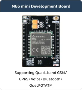
The M66 Mini DB is a compact and portable board designed specifically for breadboard.
The main equipped modules are the M66 Mini DB series wireless communication modules.
Feature List #
Module Features #
- Quad-band: 850/900/1800/1900MHz
- AT Commands: GSM 07.07, 07.05 and Enhanced AT Commands
- TCP/UDP/HTTP/FTP/PPP
- Jamming Detection
- Audio
- FOTA
- OpenCPU
- QuecFastFix
MiniDB Features #
- Compatible with BreadBoard
- On Board 2A Switching Regulator
- On Board NanoSIM(4FF) socket
- Wi-Fi BT
- GNSS active antenna circuit
Development Board Resources #
Function Description #
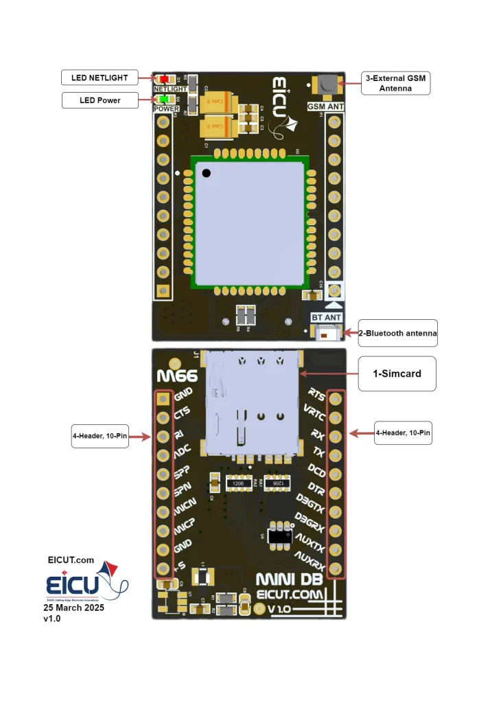
The detailed assignment of the peripheral interfaces on the Development board is as follows:

| NO. | Name | Silkscreen | Comment |
|---|---|---|---|
| 1 | Sim card case | J1 | 4FF SIM Card 12.3 × 8 mm |
| 2 | External Bluetooth Antenna | BT ANT | Johanson Bluetooth Antenna |
| 3 | External GSM Antenna | GSM ANT | UFL ANTENNA |
| 4 | 10pin | P1-P2 | Header 2.54 mm |
The Development board has 2 functional indication LEDs, as follows:
- D1: NETLIGHT
- D2: Power indication LED.
Development Board Interfaces #
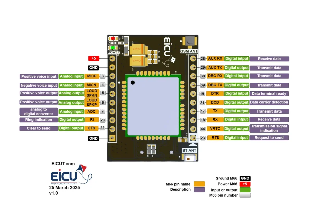
The main pin placement of the Development board is shown in the following figure:

| NO. | Name | Silkscreen | Comment |
|---|---|---|---|
| P1-1 | Request to send | RTS | You can use it as an output and input. |
| P1-2 | VRTC | VRTC | Power supply for RTC when VBAT is not supplied for the system. Charging for backup battery or golden capacitor when the VBAT is applied. For the allowed voltage and current values for this pin, see the bottom of the table. |
| P1-3 | RXD | RX | Receive data |
| P1-4 | TXD | TX | Transmit data |
| P1-5 | DCD | DCD | Digital output |
| P1-6 | DTR | DTR | Digital input |
| P1-7 | DBG-TXD | DBGTX | Transmit data |
| P1-8 | DBG-RXD | DBGRX | Receive data |
| P1-9 | TXD-AUX | AUXTX | Transmit data |
| P1-10 | RXD-AUX | AUXRX | Receive data |
| P2-1 | Ground | GND | – |
| P2-2 | CTS | CTS | Clear to send |
| P2-3 | RI | RI | Ring indication |
| P2-4 | ADC0 | ADC | General purpose analog to digital converter. Vmax=2.8V, Vmin=0V |
| P2-5 | SPK1P | SPP | Channel 1 positive voice output |
| P2-6 | SPK1N | SPN | Channel 1 negative voice output |
| P2-7 | MICN | MICN | Negative voice input |
| P2-8 | MICP | MICP | Positive voice input |
| P2-9 | Ground | GND | – |
| P2-10 | Power | +5 | Main power supply of module. Make sure that supply sufficient current in a transmitting burst typically rises to 1.6A. Vmax=4.8V, Vmin=5.5V |
VOmax=3V, VOmin=2V, VOnorm=2.8V IOmax=2mA Iin≈10uA
Development Board Dimensions #

Getting Started Preparation #
Step 1: Install Qnavigator software.
Click here to Download QNavigator Software
Step 2: After installation Act like a software wizard.
Step 3: Connect the Development Board by USB to UART converter to the computer.(pin p1-3, p1-4)
Download your driver type according to the USB-to-serial IC model
Step 4: select your board in the port section, set the baudrate to 115200, and click Connect.
Step 5: Click on the gear and see if the module is connected.
Step 6: By entering AT Command, you can use different parts of the module.
Make sure the power supply voltage is stable. The board to power up and turn on automatically without the need for a turn-off function.


