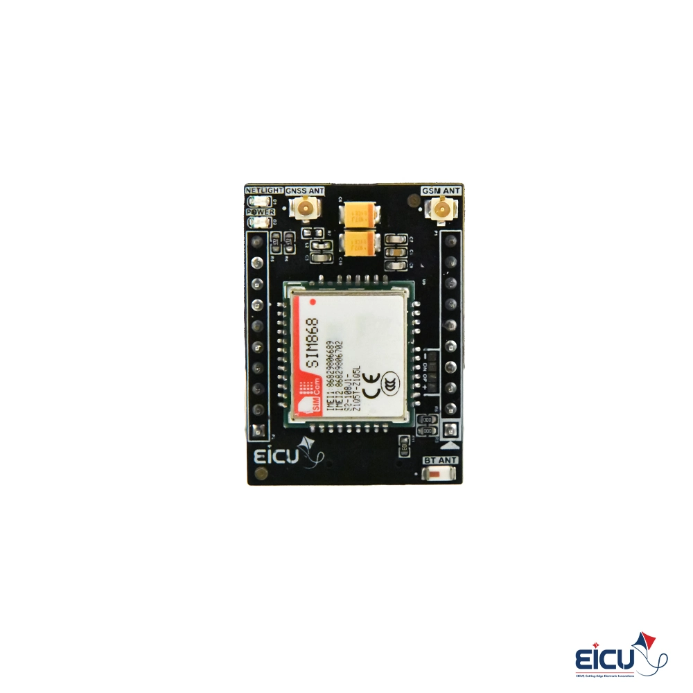
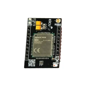
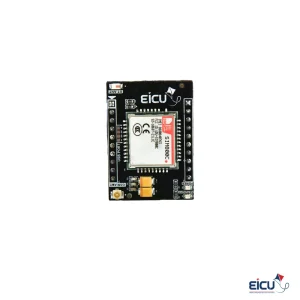
SIM868 mini Development Board for 2G/GNSS/GPS applications
- Abundant software functions: DTMF, MMS, MUX
- Low Power consumption
- Embedded TCP/UDP protocols
- Multi-constellation GNSS receiver support: GPS, GLONASS, BeiDou
$ 12.9
CompareDescription
The SIM868 Mini DB Is a compact and integrated module designed specifically to be used on products and save a lot of time handling GSM & GNSS power, RF circuits and etc. The SIM868 EVB (Evaluation Board) exposes the SIM868 module, a complete Quad‑Band GSM/GPRS cellular module with integrated GNSS (GPS/GLONASS/BDS) in an easy‑to‑use board form. The EVB presents the module’s LCC+LGA form factor and standard interfaces (UART, USB2.0, GPIO, etc.) on accessible connectors and test points, so you can prototype, integrate, and validate cellular + satellite‑navigation functions quickly without custom PCB development.
Features
- Cellular & GNSS combined: Quad‑Band GSM/GPRS plus integrated GNSS (GPS/GLONASS/BDS) on one board.
- Multiple interfaces: Exposed UART, USB2.0, GPIO and other common signals for flexible integration.
- Compact form factor: LCC+LGA module footprint supported; EVB provides pads and connectors for rapid testing.
- Easy integration: Industry‑standard interfaces and abundant extension pins simplify connecting sensors, microcontrollers, or host systems.
- Development friendly: Test points, power management, and example connections speed up evaluation and firmware development.
Specifications
- Cellular: Quad‑Band GSM/GPRS (supports standard GSM frequencies)
- GNSS: GPS, GLONASS, BDS support for accurate satellite navigation and positioning
- Interfaces: UART, USB2.0, GPIO (plus additional extension pins exposed on the EVB)
- Module package: LCC + LGA form factor (compact footprint)
- Connectivity: Designed to operate wherever cellular and GNSS signals are available
Applications
- Asset tracking and fleet management
- Portable and wearable GPS devices
- M2M/IoT telematics and remote monitoring
- Personal locators and safety devices
- Any project requiring combined cellular data and satellite positioning
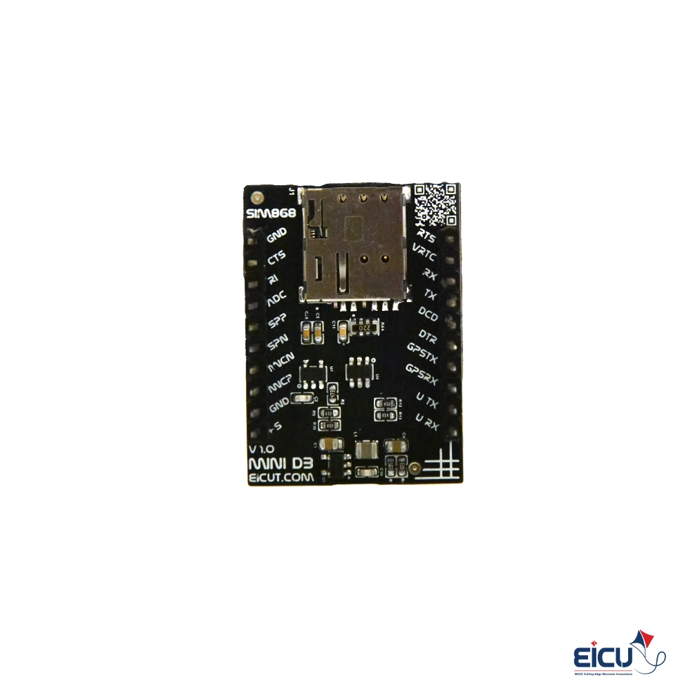
Components
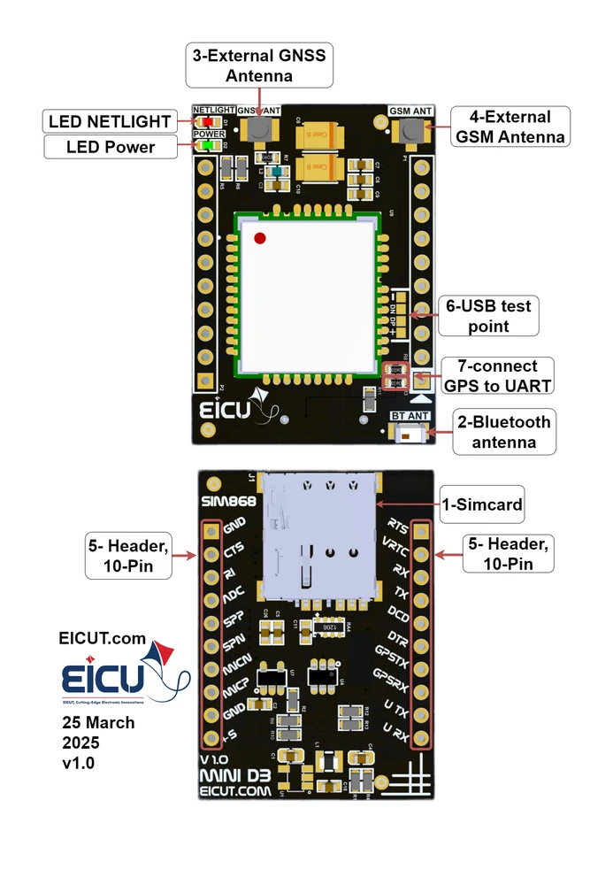
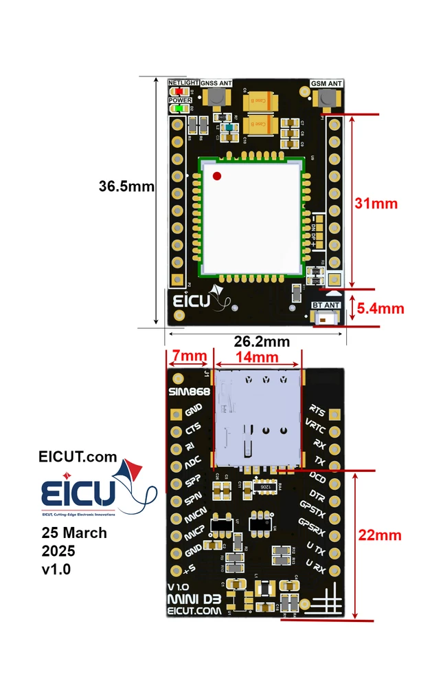
PinOut
Pin Describtion
| NO. | Name | Silkscreen | Comment |
| P1-1 | Request to send | RTS | You can use it as an output and input. |
| P1-2 | VRTC | VRTC | Power supply for RTC when VBAT is not supplied for the system. Charging for backup battery or golden capacitor when the VBAT is applied.) For the allowed voltage and current values for this pin, see the bottom of the table.) |
| P1-3 | RXD | RX | Receive data |
| P1-4 | TXD | TX | Transmit data |
| P1-5 | DCD | DCD | Digital output |
| P1-6 | DTR | DTR | Digital input |
| P1-7 | GPS-TX | GPSTX | Transmit data |
| P1-8 | GPS-RX | GPSRX | Receive data |
| P1-9 | UART-TX | U TX | Transmit data |
| P1-10 | UART-RX | U RX | Receive data |
| P2-1 | Ground | GND | |
| P2-2 | CTS | CTS | Clear to send |
| P2-3 | RI | RI | Ring indication |
| P2-4 | ADC0 | ADC | General purpose analog to digital converter. Vmax=2.8V, Vmin=0V |
| P2-5 | SPK1P | SPP | Channel 1 positive voice output |
| P2-6 | SPK1N | SPN | Channel 1 negative voice output |
| P2-7 | MICN | MICN | negative voice input |
| P2-8 | MICP | MICP | Positive voice input |
| P2-9 | Ground | GND | |
| P2-10 | Power | +5 | Main power supply of module Make sure that supply sufficient current in a transmitting burst typically rises to 1.6A. Vmax=4.8V, Vmin=5.5V |
VRTC pin voltage: VImax=3.3V, VImin=1.5V, VInorm=2.8V
VOmax=3V, VOmin=2V, VOnorm=2.8V IOmax=2mA Iin≈10uA
Hint: make sure the power supply voltage is stable. The board to power up and turn on automatically without the need for a turn-off function.
Dimentions
Benefits of using the EVB
- Faster design cycles: Validate RF, GNSS and interface integration without designing a custom PCB.
- Lower development cost: Save time and expense by using the EVB for prototyping and firmware validation.
- Easier debugging: Accessible connectors and test points make troubleshooting and signal measurement straightforward.
- Flexible experimentation: Quickly test different host controllers, power setups, or peripheral configurations.
- Seamless tracking capability: Built‑in GNSS plus industry‑standard interfaces let you track assets reliably at any location with signal coverage.
The SIM868 EVB therefore helps you develop GNSS‑enabled cellular products more easily and faster while reducing integration risk and initial cost.
Development Board Configuration
The detailed assignment of the peripheral interfaces on the Development board is as follows:
| NO. | Name | Silkscreen | Comment |
| 1 | Sim card case | J1 | 4FF SIM Card 12.3* 8mm |
| 2 | External Bluetooth Antenna | BT ANT | Johanson Bluetooth Antenna |
| 3 | External GNSS Antenna | GSM ANT | UFL ANTENNA |
| 4 | External GSM Antenna | GNSS ANT | UFL ANTENNA |
| 5 | 10pin | P1-P2 | header 2.54mm |
| 6 | USB | USB PORT | USB interface which can be used for debugging and upgrading firmware; |
| 7 | jumper | R8,R3 | Short circuit to connect the internal GPS to the internal UART module. |
The Development board has 2 functional indication LEDs, as follows:
- D1: NETLIGHT
- D2: Power indication LED
Downloads
Based on 0 reviews
Be the first to review “SIM868 mini Development Board for 2G/GNSS/GPS applications”
Related products
-
-
Development Boards
M66 mini Development Board
- Extremely compact quad-band GSM/GPRS module
- Easier soldering process with LCC package
- Power consumption as low as 1.3mA
- Support Voice, Bluetooth, QuecFOTATM and Quectel OpenCPU functions
- Embedded powerful Internet service protocols, multiple Sockets & IP addresse
SKU: E0674 -
There are no reviews yet.