

CH32V003 Mini Development Board
Out of stock
- Mini Development Board For CH32V003F4P6 From Wch
$ 5.0
Out of stock
CompareCH32V003 Mini Development Board Description
CH32V003 series is an industrial-grade general-purpose microcontroller designed based on QingKe RISC-V2Acore, which supports 48MHz system main frequency in the product function. The series features wide voltage,single line debug, low-power consumption and ultra-small package. It provides commonly used peripheralfunctions, built-in 1 group of DMA controller, 1 group of 10-bit analog-to-digital conversion ADC, 1 group ofop-amp comparator, multiple timers, standard communication interfaces such as USART, I2C, SPI, etc. The rated operating voltage of the product is 3.3V or 5V, and the operating temperature range is -40℃~85℃ industrial-grade.
Microcontroller
QingKe V2 series microprocessor is a 32-bit general-purpose MCU based on the RISC-V instruction set (RV32I subset RV32E). It uses only 16 general-purpose registers and a streamlined structure optimized for deep embedded scenarios. The V2 series supports the RV32EC extension; the V2C variant adds hardware multiplication. Custom XW extensions include Hardware Prologue/Epilogue (HPE), Vector Table Free (VTF), a simplified 1-wire/2-wire serial debug interface (SDI), and support for the WFE instruction.
CH32V003 Mini Development Board Specifications
- Core: 32-bit RISC-V (RV32EmC / RV32EC for extensions)
- Registers: 16 general-purpose registers
- Pipeline: 2-stage
- Interrupts: Up to 256 (including exceptions)
- Low-power: Sleep, Deep sleep; WFI/WFE support
- Debug interfaces: 1-wire/2-wire SDI, standard RISC-V debug
- Optional: V2C supports hardware multiplication
CH32V003 Mini Development Board Applications
- Deeply embedded systems requiring a minimal-footprint RISC-V core
- Low-power MCU applications (battery-powered sensors, wearables)
- Systems needing compact interrupt handling and fast wake/sleep transitions
- Designs that benefit from simplified debug (1-wire/2-wire SDI) and custom instruction extensions (HPE, VTF, XW)
CH32V003 Mini Development Board dimensions

Downloads
Based on 0 reviews
Be the first to review “CH32V003 Mini Development Board”
You must be logged in to post a review.
| Core | 32-bit RISC-V (RV32EmC / RV32EC for extensions) |
|---|---|
| Registers | 16 general-purpose registers |
| Pipeline | 2-stage |
| Interrupts | Up to 256 (including exceptions) |
| Low-power | Sleep, Deep sleep; WFI/WFE support |
| Debug interfaces | 1-wire/2-wire SDI, standard RISC-V debug |
Related products
-
-
-
Development Boards
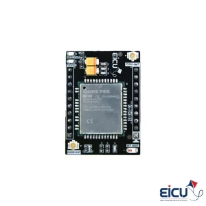
MC60 Mini Development Board Supporting Quad-band GSM/GPRS/GPS/GLONASS/QZSS/Bluetooth
 Development Boards
MC60 Mini Development Board Supporting Quad-band GSM/GPRS/GPS/GLONASS/QZSS/Bluetooth
- Multi navigation constellation: GPS/ GLONASS/ QZSS
- GNSS receiver channels: 99 acquisition/ 33 tracking channels
- Built-in LNA for better GNSS sensitivity (-167dBm@Tracking): able to use passive GNSS antenna without the need of any extra LNA
- Enhanced GNSS features: SDK command/ AIC/ LOCUS/ GLP
- GSM quad-band: 850/ 900/ 1800/ 1900MHz
- Multi internet protocols: TCP/ UDP/ PPP/ HTTP/ FTP/ SSL
- Support Voice, SMS, QuecFOTATM, DSSS, OpenCPU
- Support Bluetooth V3.0: SPP & HFP-AG profile
SKU: E0580 -
Development Boards
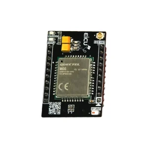
M66 mini Development Board Supporting Quad-band GSM/GPRS/Voice/Bluetooth/QuecFOTATM
 Development Boards
M66 mini Development Board Supporting Quad-band GSM/GPRS/Voice/Bluetooth/QuecFOTATM
- Extremely compact quad-band GSM/GPRS module
- Easier soldering process with LCC package
- Power consumption as low as 1.3mA
- Support Voice, Bluetooth, QuecFOTATM and Quectel OpenCPU functions
- Embedded powerful Internet service protocols, multiple Sockets & IP address
SKU: E0674
There are no reviews yet.