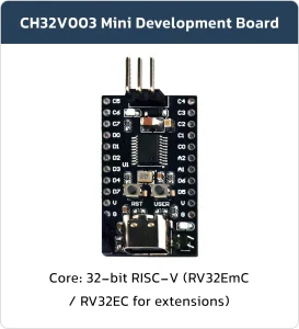
CH32V003 DB
Basic Overview #
CH32V003 series is an industrial-grade general-purpose microcontroller designed based on QingKe RISC-V2Acore, which supports 48MHz system main frequency in the product function. The series features wide voltage, single line debug, low-power consumption and ultra-small package. It provides commonly used peripheralfunctions, built-in 1 group of DMA controller, 1 group of 10-bit analog-to-digital conversion ADC, 1 group ofop-amp comparator, multiple timers, standard communication interfaces such as USART, I2C, SPI, etc. The rated operating voltage of the product is 3.3V or 5V, and the operating temperature range is -40℃~85℃ industrial-grade.
Feature List #
| Feature | Value | Unit/Note |
|---|---|---|
| Core | ||
| CPU | QingKe 32-bit RISC-V (RV32EC) | Instruction set |
| Interrupts | Fast PIC + hardware interrupt stack | — |
| Nesting | 2-level | Interrupt nesting |
| System clock | 48 | MHz main frequency |
| Memory | ||
| SRAM | 2 | KB volatile data storage |
| CodeFlash | 16 | KB program memory |
| BootLoader | 1920 | B |
| System config NVM | 64 | B non-volatile |
| User NVM | 64 | B user-defined |
| Power management & low-power | ||
| VDD | 3.3 / 5 | V supply |
| Low-power modes | Sleep, Standby | — |
| Clock & Reset | ||
| RC oscillator (HSI) | 24 | MHz, factory-trimmed |
| RC oscillator (LSI) | 128 | KHz |
| External oscillator | 4–25 | MHz high-speed crystal |
| Reset/voltage | POR/PDR + PVD | Power on/down reset, programmable voltage detector |
| DMA & Analog | ||
| DMA | 1 group, 7 channels | Ring buffer; TIMx/ADC/USART/I2C/SPI |
| OPA & comparator | 1 group | Connected to ADC & TIM2 |
| ADC | 10-bit | 0–VDD; 8 external + 2 internal; external delayed trigger |
| Timers | ||
| Advanced timer | 1 × 16-bit | Dead-zone, emergency brake, complementary PWM |
| General-purpose timer | 1 × 16-bit | IC/OC/PWM/pulse counting/incremental encoder |
| Watchdogs | 2 | Independent + window watchdog |
| SysTick | 32-bit | Counter |
| Communication interfaces | ||
| USART | 1 | — |
| I2C | 1 | — |
| SPI | 1 | — |
| GPIO | ||
| Ports | 3 groups / 18 I/O | — |
| EXTI | 1 | Mapped external interrupt |
| Security / Debug / Package | ||
| Unique ID | 64-bit | — |
| Debug | 1-wire SDI | Serial debug interface |
| Package | SOP / TSSOP / QFN | — |
Board Resources #
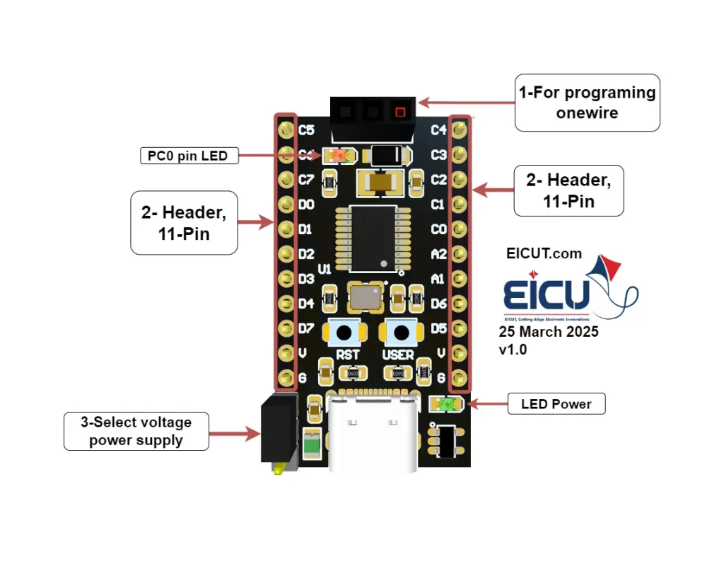
Function Description #
The detailed assignment of the peripheral interfaces on the Development board is as follows:
| NO. | Name | Silkscreen | Comment |
|---|---|---|---|
| 1 | Programing pin | – | You can program the development board with the one-wire protocol. |
| 2 | 11 pin | – | Ch32v Output pin |
| 3 | 3 pin | – | select voltage power supply 3.3V,5V |
The Development board has 2 functional indication LEDs, as follows:
- Connect to PC0(10) pin wch.
- Power indication LED.
Development Board Interfaces #
The main pin placement of the Development board is shown in the following figure:
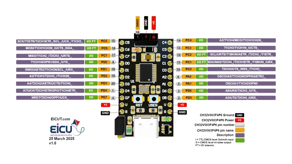
| SOP16 | TSSOP20 | QFN20 | SOP8 | Pin name | Pin type (1) | I/O structure | Main function (after reset) | Default alternate function |
|---|---|---|---|---|---|---|---|---|
| – | – | 0 | – | VSS | P | VSS | – | – |
| 8 | 1 | 18 | 8 | PD4 | I/O | PD4 | UCK/T2CH1ETR/A7/OPO | TICH4ETR_(1) |
| 9 | 2 | 19 | 8 | PD5 | I/O | PD5 | UTX/A5 | T2CH4_/URX_ |
| 10 | 3 | 20 | 1 | PD6 | I/O | PD6 | URX/A6 | T2CH3_/UTX_ |
| 11 | 4 | 1 | – | PD7 | I/O | PD7 | NRST/T2CH4/OPP1 | UCK_ |
| 12 | 5 | 2 | 1 | PA1 | I/O | PA1 | T1CH2/A1/OPN0 | OSCI |
| 13 | 6 | 3 | 3 | PA2 | I/O | PA2 | TICH2N/A0/OPP0 | OSCO/AETR2_ |
| 14 | 7 | 4 | 2 | VSS | P | VSS | – | – |
| – | 8 | 5 | – | PD0 | I/O | PD0 | TICH1N/OPN1 | SDA_/UTX_ |
| 15 | 9 | 6 | 4 | VDD | P | VDD | – | – |
| 16 | 10 | 7 | – | PC0 | I/O | PC0 | T2CH3 | NSS_/UTX_/T1CH3_ |
| 1 | 11 | 8 | 5 | PC1 | I/O/FT | PC1 | SDA/NSS | T1BKIN_/T2CH4_/T2CH1ETR_/URX_ |
| 2 | 12 | 9 | 6 | PC2 | I/O/FT | PC2 | SCL/URTS/T1BKIN | AETR_/T2CH2_/T1ETR_ |
| 3 | 13 | 10 | – | PC3 | I/O | PC3 | T1CH3 | T1CH1N_/UCTS_ |
| 4 | 14 | 11 | 7 | PC4 | I/O | PC4 | T1CH4/MCO/A2 | T1CH1CH2N_(2) |
| – | 15 | 12 | – | PC5 | I/O/FT | PC5 | SCK/T1ETR | T2CH1ETR_/SCL_/UCK_/T1CH3_ |
| 5 | 16 | 13 | – | PC6 | I/O/FT | PC6 | MOSI | T1CH1CH3N_(3)/UCTS_/SDA_ |
| 6 | 17 | 14 | – | PC7 | I/O | PC7 | MISO | T1CH2_/URTS_/T2CH2_ |
| 7 | 18 | 15 | 8 | PD1 | I/O | PD1 | SWIO/T1CH3N/AETR2 | SCL_/URX_ |
| – | 19 | 16 | – | PD2 | I/O | PD2 | T1CH1/A3 | T2CH3_/T1CH2N_ |
| – | 20 | 17 | – | PD3 | I/O | PD3 | A4/T2CH2/AETR/UCTS | T1CH4_ |
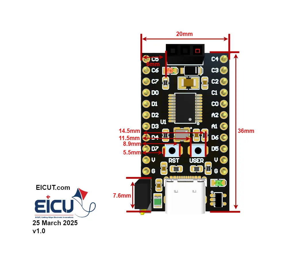
Development Board Dimensions #
Getting Started Preparation #
To program this series of RISC_V microcontrollers, we use the MounRiver Studio software, abbreviated as MRS.
To download this IDE, you can visit the MounRiver Studio website below
This IDE has the ability to program WCH chips internally; but if you want to use external software for programming, you can use the WCH-LinkUtility software, which can be downloaded from the WCH company website.
To connect the programmer to the micro, the GND -> GND and SWDIO -> SWDIO and +5 -> VDD pins must be connected together. If the circuit connected to the micro draws a small current, you can supply the IC power from the programmer itself.
Resource Download #
FAQ #