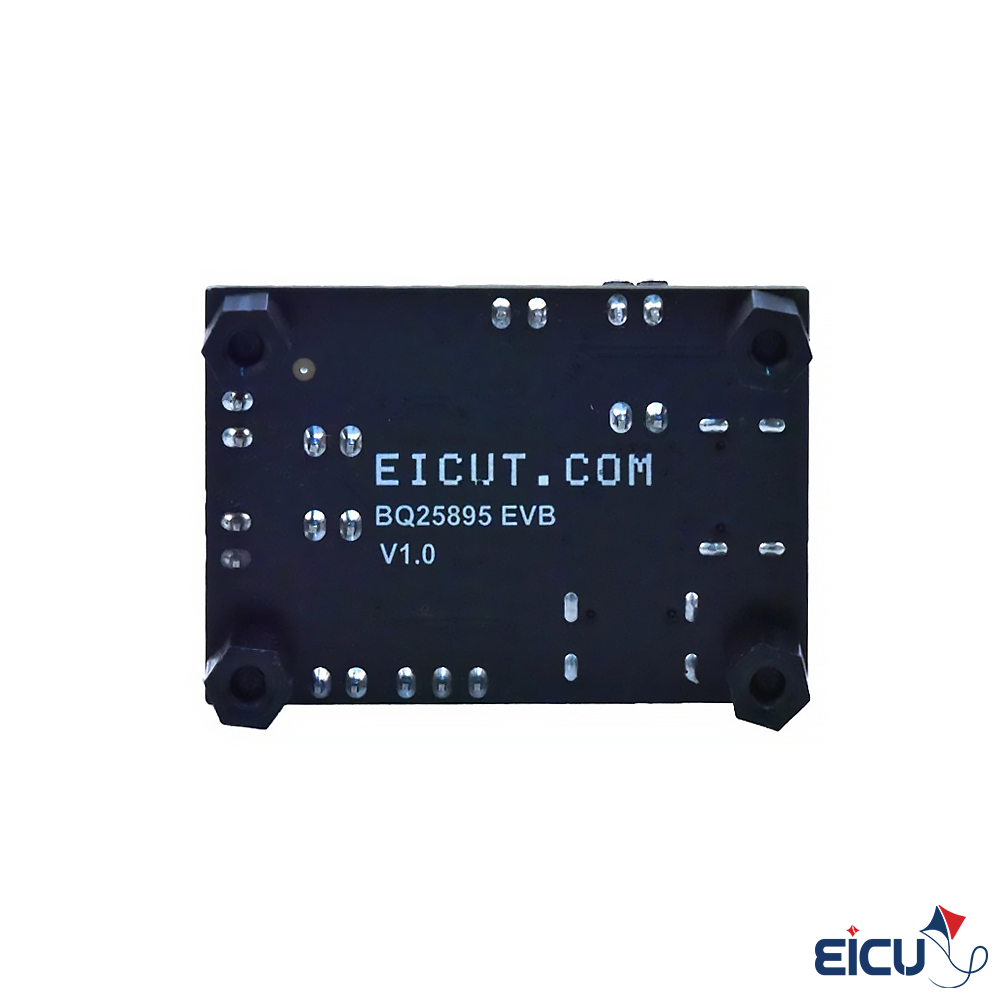
TI BQ25895 Mini DB – Fast Charger
10 in stock
- High efficiency 5-A, 1.5-MHz switch mode buck charge
- Charger current: up to 5 A (1.5 MHz buck)
- Boost output: adjustable 4.5–5.5 V, up to 3.1 A (500 kHz–1.5 MHz selectable)
- Input voltage range: 3.9–14 V
$ 9.5
10 in stock
TI BQ25895 Mini DB Description
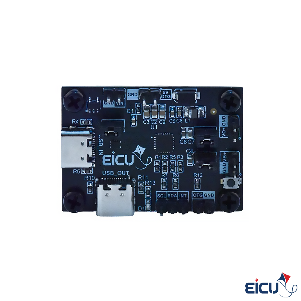
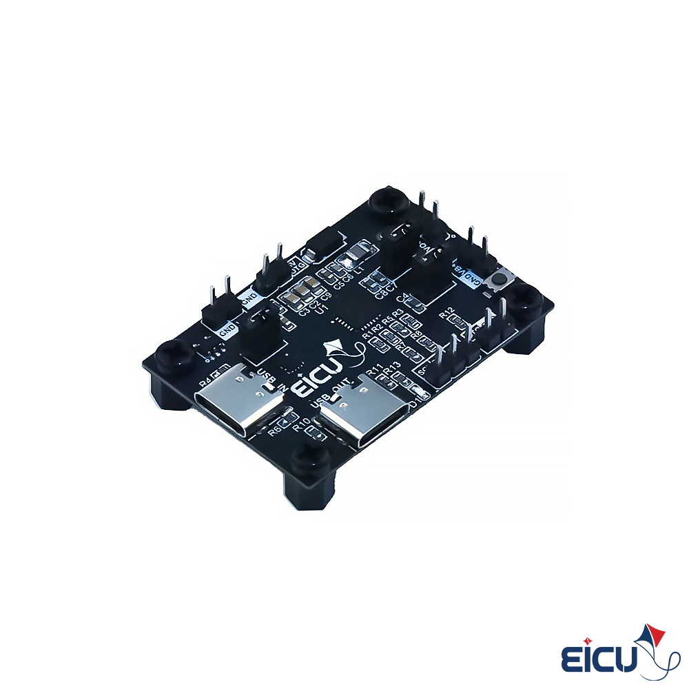
The Mini Development Board (MiniDB) integrates the BQ25895 — a highly integrated 5-A switch‑mode battery charge-management and system power‑path device for single‑cell Li‑Ion/Li‑polymer batteries. It supports high‑input‑voltage fast charging and combines low‑impedance power‑path management to improve efficiency, reduce charge time, and extend battery life during discharge. The MiniDB exposes the module’s pins and I²C control so designers can prototype quickly without designing the full power subsystem.
TI BQ25895 Mini DB Features
- High‑efficiency 5-A, 1.5‑MHz switch‑mode buck charger (up to 93% charge efficiency at 2 A; 91% at 3 A)
- Optimized for high input voltages (9–12 V) with Low‑Power PFM mode for light loads
- Boost mode with adjustable output 4.5–5.5 V and selectable 500 kHz–1.5 MHz switching (up to 3.1 A, 93% boost efficiency at 5 V @ 1 A)
- Integrated automatic switch between Charge and Boost modes
- Single input supporting USB and high‑voltage adapters (3.9–14 V) with input current limit 100 mA–3.25 A (50 mA steps)
- Auto‑detects USB SDP, CDP, DCP and non‑standard adapters; Maximum Power Tracking (input voltage limit up to 14 V)
- Input Current Optimizer (ICO) to maximize input power without overloading adapters
- Resistance compensation (IRCOMP) from charger output to cell terminal
- Low‑resistance BATFET and discharge MOSFET (11 mΩ) for high battery discharge efficiency (up to 9 A)
- Integrated ADC for system monitoring (voltage, temperature, charge current)
- Narrow VDC (NVDC) power‑path: instant‑on with no or deeply discharged battery; ideal‑diode behavior in Battery Supplement Mode
- BATFET control for Ship Mode, wake‑up, and system reset
- Flexible autonomous and I²C control modes for optimal performance
- High integration (all MOSFETs, current sensing, loop compensation included)
- Ultra‑low 12‑µA battery leakage for Ship Mode
- High accuracy: ±0.5% charge voltage, ±5% charge current, ±7.5% input current regulation
- Safety features: battery temperature sensing, thermal regulation and thermal shutdown
TI BQ25895 Specifications
| Parameter | Test Conditions | Min | Typ | Max | Unit |
|---|---|---|---|---|---|
| IBAT Battery discharge current (BAT, SW, SYS) in buck mode |
VBUS = 4.2 V, V(VBUS) < V(UVLO), leakage between BAT and VBUS | — | 5 | — | µA |
| High-Z mode, no VBUS, BATFET disabled (REG09[5]=1), battery monitor disabled, TJ < 85°C | 12 | — | 23 | ||
| High-Z mode, no VBUS, BATFET enabled (REG09[5]=0), battery monitor disabled, TJ < 85°C | 32 | — | 60 | ||
| I(VBUS_HIZ) Input supply current (VBUS) in buck mode when High-Z mode is enabled |
V(VBUS)= 5 V, High-Z mode, no battery, battery monitor disabled | 15 | — | 35 | µA |
| V(VBUS)= 12 V, High-Z mode, no battery, battery monitor disabled | 25 | — | 50 | ||
| I(VBUS) Input supply current (VBUS) in buck mode |
VBUS > V(UVLO), VBUS > VBAT, converter not switching | 1.5 | — | 3 | mA |
| VBUS > V(UVLO), VBUS > VBAT, converter switching, VBAT = 3.2 V, ISYS = 0A | 3 | — | — | ||
| VBUS > V(UVLO), VBUS > VBAT, converter switching, VBAT = 3.8 V, ISYS = 0 A | 3 | — | — | ||
| I(BOOST) Battery discharge current in boost mode |
VBAT = 4.2 V, boost mode, I(VBUS)= 0 A, converter switching | 5 | — | — | mA |
| V(VBUS_OP) | VBUS operating range | 3.9 | — | 14 | V |
| V(VBUS_UVLOZ) | VBUS for active I2C, no battery | — | 3.6 | — | V |
| V(SLEEP) | Sleep mode falling threshold | 25 | 65 | 120 | mV |
| V(SLEEPZ) | Sleep mode rising threshold | 130 | 250 | 370 | mV |
| V(ACOV) | VBUS over-voltage rising threshold | — | 14 | 14.6 | V |
| V(ACOV falling) | VBUS over-voltage falling threshold | 13.5 | — | 14 | V |
| VBAT(UVLOZ) | Battery for active I2C, no VBUS | — | 2.3 | — | V |
| VBAT(DPL) | Battery depletion falling threshold | 2.15 | 2.5 | — | V |
| VBAT(DPLZ) | Battery depletion rising threshold | 2.35 | 2.7 | — | V |
| V(VBUSMIN) | Bad adapter detection threshold | — | 3.8 | — | V |
| I(BADSRC) | Bad adapter detection current source | — | 30 | — | mA |
| VSYS Typical system regulation voltage |
I(SYS) = 0 A, VBAT > VSYS(MIN), BATFET Disabled (REG09[5]=1) | VBAT + 50 mV | — | — | V |
| I(SYS) = 0 A, VBAT < VSYS(MIN), BATFET Disabled (REG09[5]=1) | VSYS(MIN) + 150 mV | — | — | ||
| VSYS(MIN) | Minimum DC system voltage output | VBAT < VSYS(MIN), SYS_MIN = 3.5 V (REG03[3:1]=101), ISYS= 0 A | 3.50 | 3.65 | V |
| VSYS(MAX) | Maximum DC system voltage output | VBAT = 4.35 V, SYS_MIN = 3.5V (REG03[3:1]=101), ISYS= 0 A | 4.40 | 4.42 | V |
TI BQ25895 Mini DB Applications
- Power banks and portable chargers
- Mobile Wi‑Fi hotspots
- Wireless Bluetooth speakers
- Portable internet and handheld devices
Benefits for Design and Prototyping
- Speeds development: exposing the BQ25895 functions on a MiniDB removes the need to design a complete charging/power‑path circuit from scratch.
- Easier I²C control and monitoring for system integration and tuning.
- Safer, more reliable prototypes thanks to integrated protections (thermal, temperature sensing, input current optimization).
- Compact, high‑efficiency solution that reduces board space and BOM complexity while improving battery life and charge times.
Downloads
| Charger current | up to 5 A (1.5 MHz buck) |
|---|---|
| Boost output | adjustable 4.5–5.5 V, up to 3.1 A (500 kHz–1.5 MHz selectable) |
| Input voltage range | 3.9–14 V |
| Input current limit range | 100 mA–3.25 A (50 mA resolution) |
| Battery discharge MOSFET RDS(on) | ~11 mΩ (supports up to 9 A) |
| Leakage (Ship Mode) | 12 µA |
| Regulation accuracy | ±0.5% VCHG, ±5% ICHG, ±7.5% IIN |
| Integrated peripherals | ADC (voltage, temperature, charge current), I²C interface, BATFET control |
Based on 0 reviews
Be the first to review “TI BQ25895 Mini DB – Fast Charger”
You must be logged in to post a review.
There are no reviews yet.