FSA2568 Dual Sim Card Analoge Switch, for 2FF USIM, FPC Cable support
- Dual‑SIM switching EVB using FSA2567 fast, reliable
- Easier debugging
- Firmware integration
- Low‑loss supply switching
- High‑speed data support (>160 MHz)
- Easy ESD and reliability testing
$ 3.9
CompareDescription
The FSA2567 Evaluation Board (EVB) showcases the FSA2567, a bi‑directional, low‑power, dual double‑pole double‑throw (4PDT) analog switch designed for dual‑SIM card multiplexing. The device is optimized for switching WLAN–SIM data and control signals and includes a dedicated channel for the SIM supply path. Special low‑power circuitry reduces current consumption when the SEL control voltage is lower than VCC, enabling direct interface with baseband GPIOs in ultra‑portable devices.
Features
- Low on‑capacitance (data path): 10 pF typical for high‑speed data transfer
- Low on‑resistance (data path): 6 Ω typical
- Low on‑resistance (supply path): 0.4 Ω typical to minimize voltage drop on SIM supply
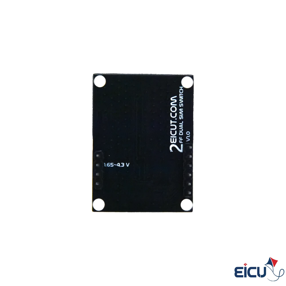
- Wide VCC range: 1.65 V to 4.3 V
- Low power consumption: 1 μA maximum (typical); up to 15 μA ICCT across expanded range (VIN = 1.8 V, VCC = 4.3 V)
- High bandwidth: >160 MHz (-3 dB)
- Packages available: Pb‑free 16‑lead MLP and 16‑lead UMLP
- ESD protection: 3 kV signal ESD rating; >12 kV power/GND ESD rating
Specifications
- Topology: Dual 4PDT analog switch (bi‑directional)
- Data path CON: 10 pF (typical)
- Data path RON: 6 Ω (typical)
- Supply path RON: 0.4 Ω (typical)
- VCC operating range: 1.65–4.3 V
- Quiescent/current consumption: 1 μA max (normal), 15 μA max ICCT under expanded conditions
- Bandwidth: >160 MHz (-3 dB)
- Package options: 16‑lead MLP, 16‑lead UMLP (Pb‑free)
- ESD ratings: 3 kV (signal), >12 kV (power/GND)
Applications
- Cell phones and dual‑SIM handsets
- PDAs and smartphones
- Digital cameras and portable consumer devices
- Notebooks and printers
- LCD monitors, TVs, and set‑top boxes
- Any design requiring SIM switching, connector sharing, or low‑loss supply switching
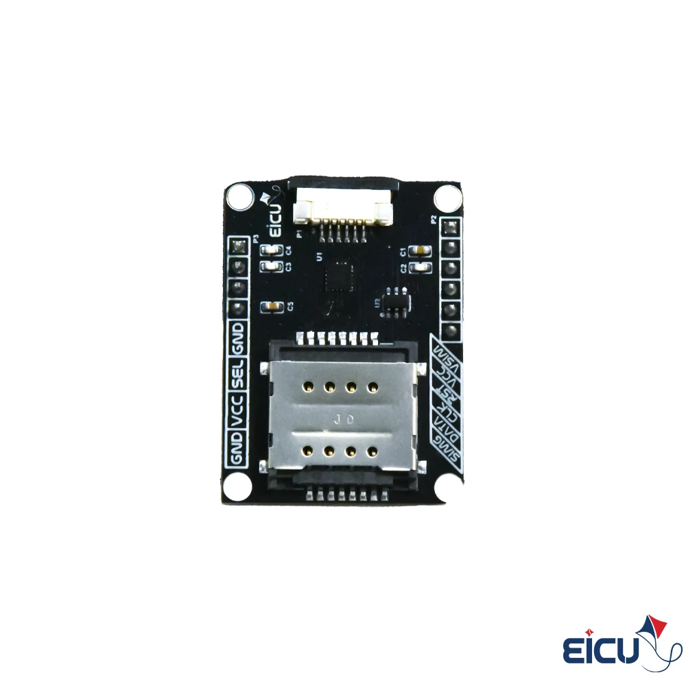
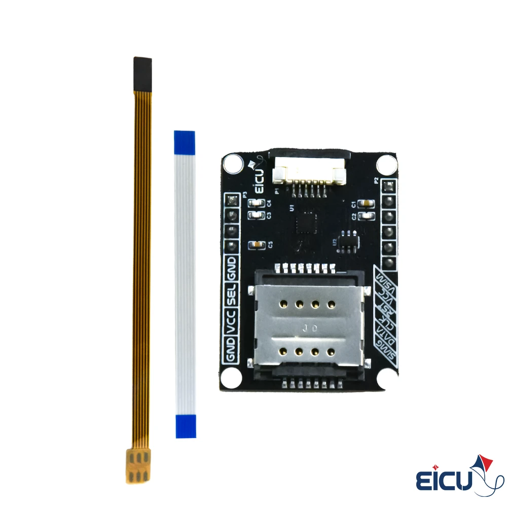
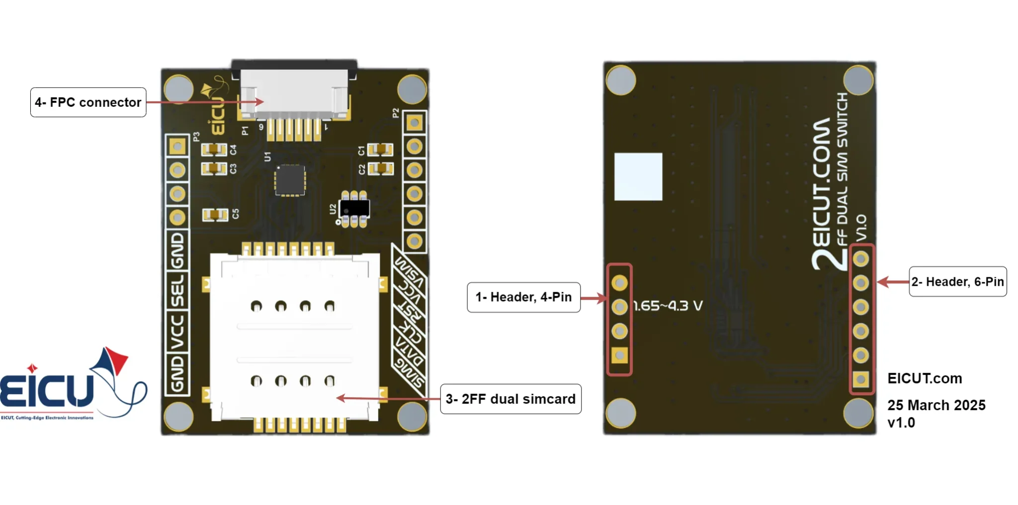
Development Board Configuration
The detailed assignment of the peripheral interfaces on the Development board is as follows:
| NO. | Name | Silkscreen | Comment |
| 1 | 4pin | P3 | header 2.54mm |
| 2 | 6pin | P2 | header 2.54mm |
| 3 | Dual Sim card case | – | 2FF SIM Card |
| 4 | FPC Connector | P1 | FPC 6pin |
DB Pionut
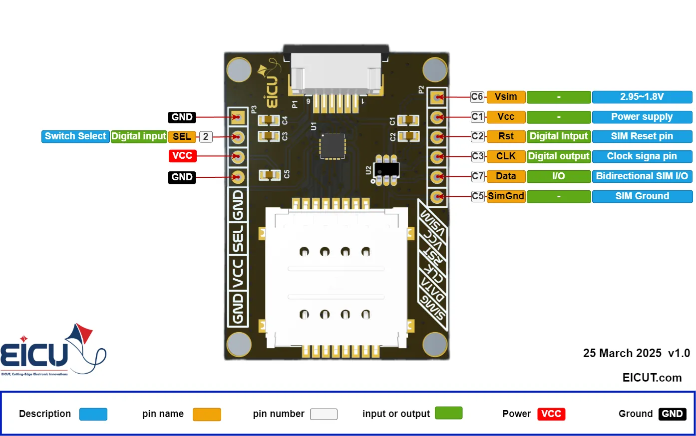
Pin Describtion
| NO. | Name | Silkscreen | Comment |
| P3-1 | Ground | GND | |
| P3-2 | Select | Sel | 0 – Power |
| P3-3 | Power | VCC | 1.65~4.3V |
| P3-4 | Ground | GND | |
| P2-1 | VSIM | VSIM | These pins are similar to the pins of the
FPC connector. You can use them if you do not use the FPC connector. |
| P2-2 | VCC | VCC | |
| P2-3 | RST | RST | |
| P2-4 | CLK | CLK | |
| P2-5 | DATA | DATA | |
| P2-6 | Simcard-GND | SIMG |
For switching between two SIM cards, you can connect the Select pin (pin header P3) to ground or VCC manually with a jumper, or you can control this pin using a microcontroller to set it high or low.
Connections
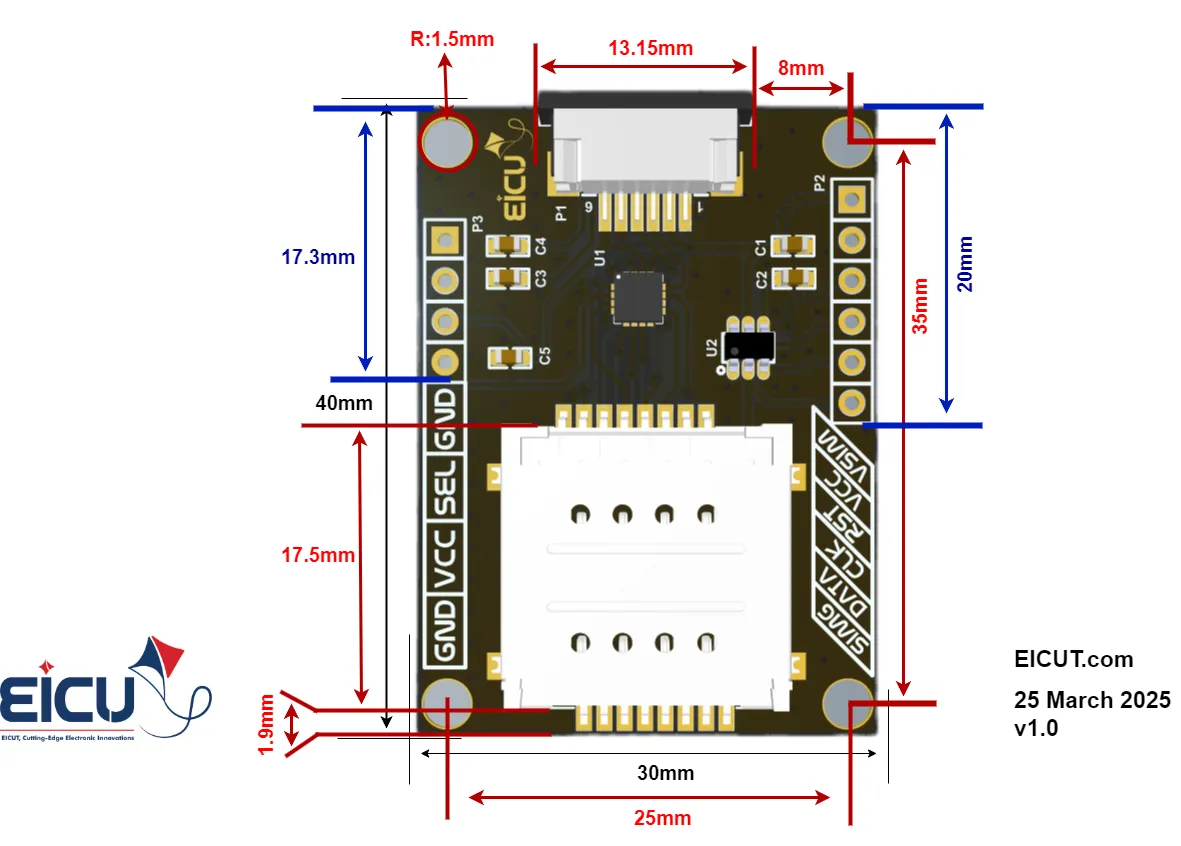
Dimentions
EVB – Faster, Easier Design
Using the FSA2567 EVB accelerates development by providing a ready‑made reference layout, validated routing for signal and supply paths, and easy access to device pins for testing. Benefits include:
- Rapid evaluation of data‑path performance (CON, RON, bandwidth) without PCB redesign
- Quick verification of supply‑path voltage drop and ESD robustness
- Simplified firmware and control testing via exposed SEL and control pins
- Reduced development risk and shorter prototype cycles through a proven reference design
Getting Started Preparation
- Step 1: Connect the board power
- Step 2: Place the SIM cards in the SIM card case
- Step 3: Switch between SIM cards by High and Low the select pin
- Step 4: Connect the board to your microcontroller with the FPC connector or the header pin(P2)
Downloads
Based on 0 reviews
Be the first to review “FSA2568 Dual Sim Card Analoge Switch, for 2FF USIM, FPC Cable support”
Related products
-
-
Development Boards
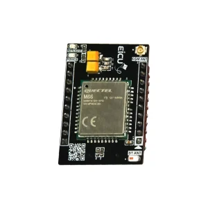
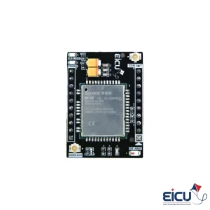
M66 mini Development Board
- Extremely compact quad-band GSM/GPRS module
- Easier soldering process with LCC package
- Power consumption as low as 1.3mA
- Support Voice, Bluetooth, QuecFOTATM and Quectel OpenCPU functions
- Embedded powerful Internet service protocols, multiple Sockets & IP addresse
SKU: E0674 -
Development Boards
MC60 Mini Development Board
- Multi navigation constellation: GPS/ GLONASS/ QZSS
- GNSS receiver channels: 99 acquisition/ 33 tracking channels
- Built-in LNA for better GNSS sensitivity (-167dBm@Tracking): able to use passive GNSS antenna without the need of any extra LNA
- Enhanced GNSS features: SDK command/ AIC/ LOCUS/ GLP
- GSM quad-band: 850/ 900/ 1800/ 1900MHz
- Multi internet protocols: TCP/ UDP/ PPP/ HTTP/ FTP/ SSL
- Support Voice, SMS, QuecFOTATM, DSSS, OpenCPU
- Support Bluetooth V3.0: SPP & HFP-AG profile
SKU: E0580
There are no reviews yet.