-
×
 M66 Development Board
1 × $ 34.9
M66 Development Board
1 × $ 34.9 -
×
 M66 open cpu IOT Development Board
1 × $ 39.5
M66 open cpu IOT Development Board
1 × $ 39.5
Subtotal: $ 74.4
$ 19.9
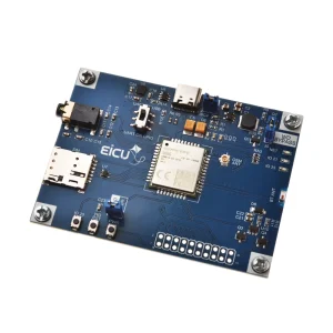
CompareThe Development Board is a versatile and feature-rich development platform, making it an excellent choice for working with the EC200 module. It is designed to facilitate IoT prototyping and supports various applications, including smart home solutions, thanks to its integrated connectivity options and modular design.
The detailed assignment of the peripheral interfaces on the Development board is as follows:
| NO. | Name | Silkscreen | Comment |
| 1 | Simcard1 case | SIM1 | 4FF SIM Card 12.3* 8mm |
| 2 | Simcard2 case | SIM2 | MFF2 SIM Card |
| 3 | USB TYPE-C | USB1 | USB interface which can be used for debugging and upgrading firmware |
| 4 | USB VBUS | U VBUS/VBUS | USB insertion detection |
| 5 | Pin header 13 pin | – | header 2.54mm |
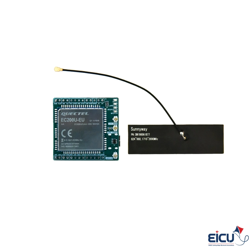
| 6 | External WIFI/Bluetooth Antenna | BT/WIFI | UFL ANTENNA |
| 7 | External GNSS Antenna | GNSS ANT | UFL ANTENNA |
| 8 | External GSM Antenna | MAIN ANT | UFL ANTENNA |
The Development board has 4 functional indication LEDs, as follows:
The main pin placement of the Development board is shown in the following figure:
| NO. | Name | Silkscreen | Comment | Interface |
| P1-1 | LOUDSPK_N | SP- | Microphone analog input (-) | Analog |
| P1-2 | LOUDSPK_P | SP+ | Loudspeaker differential output(+) | Audio |
| P1-3 | MIC_N | MIC- | Microphone analog input (-) | Analog |
| P1-4 | MIC_P | MIC+ | Microphone analog input (+) | Audio |
| P1-5 | USB_BOOT | USB | The USB_BOOT cannot be pulled up before startup and it can be used as KEYIN0 after startup. | |
| P1-6 | RESET_N | RST | Reset the module | |
| P1-7 | PWRKEY | PWR | Turn on/off the module | |
| P1-8 | ADC0 | ADC | General-purpose ADC interface | |
| P1-9 | SDIO1_DATA | DATA | SDIO data bit 0 | |
| P1-10 | SDIO1_CLK | CLK | SDIO clock | SD Card |
| P1-11 | SDIO1_CMD | CMD | SDIO command | |
| P1-12 | SDIO1_VDD | VDD | SDIO power supply | |
| P1-13 | GND | Ground | ||
| P2-1 | DEBUG_RXD | DBG RX | DEBUG Serial port receiving | Debug |
| P2-2 | DEBUG TXD | DBG TX | DEBUG Serial port sending | UART |
| P2-3 | MAIN TX | TX | The module sends data. Used for AT commands. | Main |
| P2-4 | MAIN RX | RX | The module receives data. Used for AT commands. | UART |
| P2-5 | SPI_CS | CS | SPI chip select | |
| P2-6 | SPI_MOSI | DOUT | SPI master mode output | SPI |
| P2-7 | SPI_MISO | DIN | SPI master mode input | |
| P2-8 | SPI_CLK | CLK | SPI clock | |
| P2-9 | I2C_SCL | SCL | I2C serial clock | I2C |
| P2-10 | I2C_SDA | SDA | I2C serial data | |
| P2-11 | GND | Ground | ||
| P2-12 | Power +5 | +5 | ||
| P2-13 | Power +5 | +5 |
Hint: make sure the power supply voltage is stable.
Select at least 2 products
to compare
There are no reviews yet.