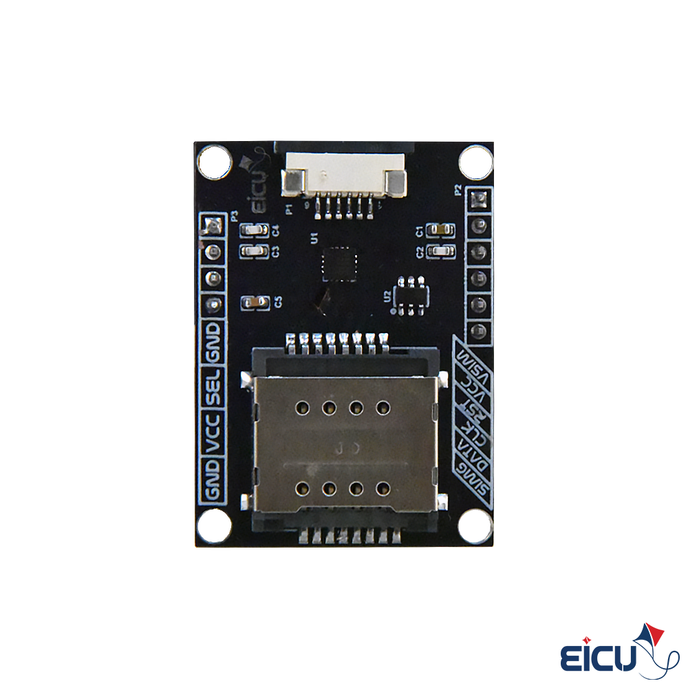
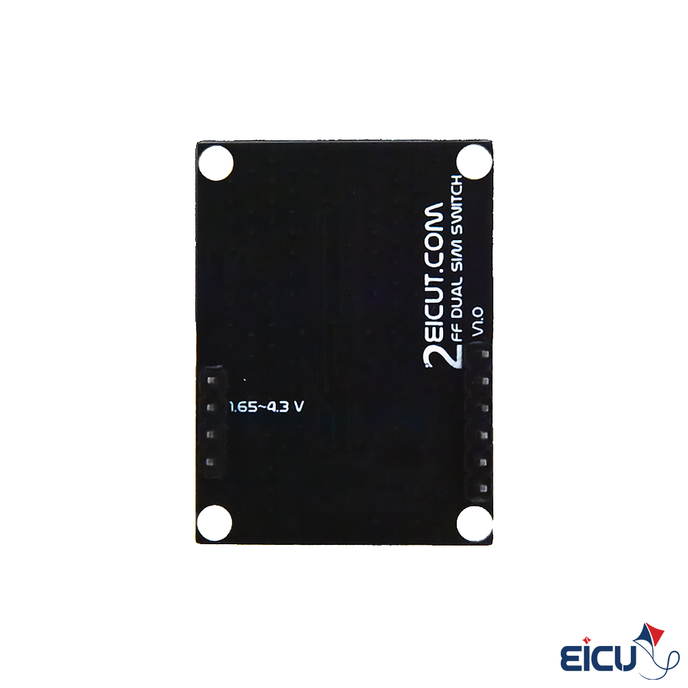
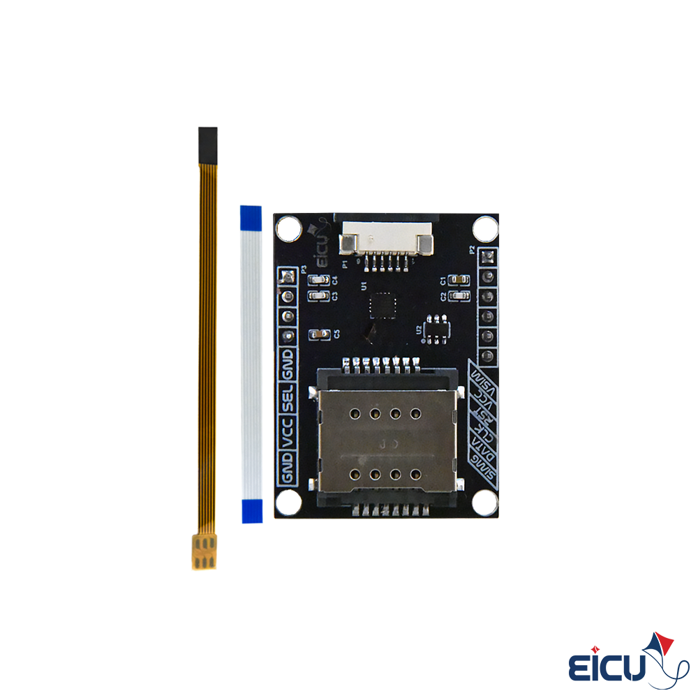
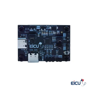
DIO1568 Dual Sim Analog Switch for 2FF USIM, FPC Cable support
10 in stock
- Ultra-low on-resistance: 0.85 Ω on SIM path
- 2FF Sim card Connector
- Very low power consumption
- Dual-SIM card multiplexing target application
$ 4.5
10 in stock
DIO1568 Dual Sim Analog Switch Description
The DIO1568 Dual Sim Analog Switch lets you quickly evaluate and prototype with the DIO1568 low-power, dual-SIM analog switch. The DIO1568 is a quad SPDT analog switch optimized for dual-SIM card multiplexing, operating from a single 1.65 V to 5.5 V supply. It offers ultra-low on-resistance (0.85 Ω on the SIM path) and fast, break-before-make switching thanks to sub-micron CMOS fabrication. The device also maintains very low quiescent current even when control voltage is below VCC, enabling direct interfacing with baseband processor GPIOs in mobile handsets. Two compact QFN package options are available: QFN1.8×2.6-16 and QFN3×3-16.
DIO1568 Dual Sim Analog Switch Features
- Switch type: Quad SPDT (4×)
- Supply voltage: 1.65 V to 5.5 V
- Low on-resistance: 0.85 Ω (SIM path); 2.7 Ω (other paths)
- Capacitance: 20 pF CON at DAT/CLK/RST path
- Low quiescent power consumption (suitable for battery-powered devices)
- Package options: 16‑lead QFN 1.8×2.6 mm and 16‑lead QFN 3×3 mm
DIO1568 Dual Sim Analog Switch Specifications
| Symbol | Parameter | Conditions | VCC (V) | Temp | Min | Typ | Max | Unit |
|---|---|---|---|---|---|---|---|---|
| VIH | Input voltage high | — | 1.65 to 4.5 | -40 to 85°C | 0.9 | — | — | V |
| VIH | Input voltage high | — | 1.65 to 4.5 | 25°C | 0.8 | — | — | V |
| VIL | Input voltage low | — | 1.65 to 4.5 | -40 to 85°C | — | — | 0.4 | V |
| IIN | Control input leakage | VSW = 0 to VCC | 4.5 | 25°C | -1 | — | 1 | µA |
| INC(OFF), INO(OFF) | Off leakage current | RSTn, DATn, CLKn, SIMn = 0.3 or 3.6 V | 4.5 | 25°C | -1 | — | 1 | µA |
| INC(ON), INO(ON) | ON leakage current | RSTn, DATn, CLKn, SIMn = 0.3 or 3.6 V | 4.5 | 25°C | -1 | — | 1 | µA |
| ICC | Quiescent supply current | VIN = 0 V or VCC, IOUT = 0 V | 4.5 | 25°C | — | 0.6 | 1.0 | µA |
| ROND | RST, DAT, CLK resistance | IOUT = -20 mA, VSW = 2.3 V | 2.7 | -40 to 85°C | — | — | 2.7 | Ω |
| RONS | SIM resistance | IOUT = -100 mA, VSW = 2.3 V | 2.7 | -40 to 85°C | — | — | 0.85 | Ω |
| ΔRON | Delta on resistance | VSW = 0 V, ION = -20 mA | 2.7 | -40 to 85°C | — | 0.2 | — | Ω |
| RFLAT(ON) | On resistance flatness | IOUT = 100 mA, RSTn, CLKn, SIMn = 0 to VCC | 2.7 | -40 to 85°C | — | — | 0.8 | Ω |
| ΔICC | Increase in ICC current per control voltage and VCC | VIN = 0.8 V | 4.5 | 25°C | — | 1 | — | µA |
| VIN = 1.5 V | 4.5 | 25°C | — | 0.61 | — |
DIO1568 Dual Sim Analog Switch Applications
- Cell phones and PDAs (dual-SIM designs)
- Set-top boxes
- Digital cameras
- Notebooks and laptops
- TV / LCD monitors
How the EVB Helps — Faster, Easier Design
- Rapid evaluation of electrical performance (on-resistance, switching, leakage) without PCB redesign.
- Reference layout and footprint for the QFN packages remove guesswork and speed board bring-up.
- Breakout connections for SIM DAT/CLK/RST and control pins allow quick functional tests and firmware integration.
- Pre-routed decoupling and recommended component placements reduce signal issues and shorten debug time.
- Demonstrates low-power behavior and direct GPIO interfacing to confirm compatibility with target baseband processors.
Use the DIO1568 EVB to accelerate prototyping, validate performance in your target system, and shorten the path from concept to final design.
Downloads
| Topology | 4× SPDT analog switch |
|---|---|
| Operating voltage range | 1.65–5.5 V |
| Quiescent current | Very low, remains low when control voltage < VCC |
| On-resistance | 0.85 Ω (SIM path) / 2.7 Ω (other paths) |
| Input/output capacitance | ~20 pF on DAT/CLK/RST lines |
| Packages | QFN1.8×2.6-16, QFN3×3-16 |
Based on 0 reviews
Be the first to review “DIO1568 Dual Sim Analog Switch for 2FF USIM, FPC Cable support”
You must be logged in to post a review.
There are no reviews yet.